
Recent technological innovations like 5G connectivity, internet-of-things sensors and artificial intelligence have helped printed-circuit–board (PCB) manufacturing gain a significant impetus, but there are still a few challenges to address.
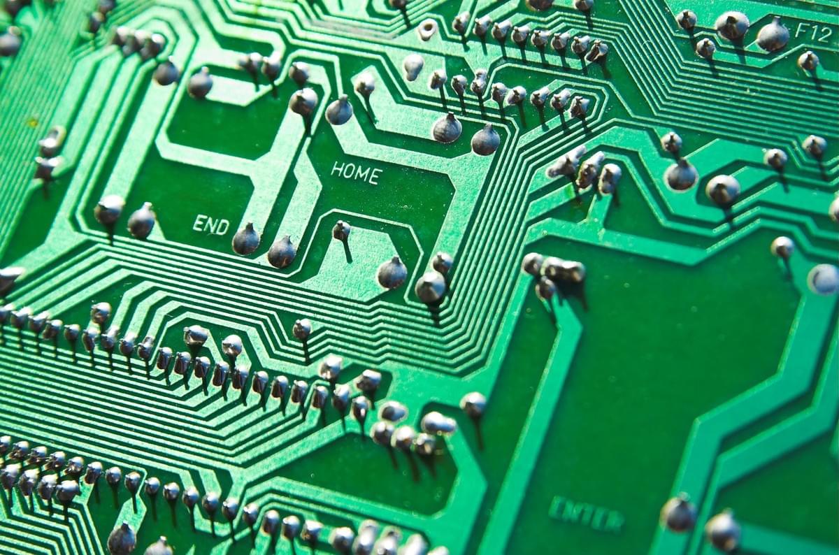
In the past, manufacturing circuit boards was done either by additive or subtractive methods. But product designers and contract manufacturers soon recognized the benefits of using both types in a hybrid process. The additive method’s quick turnaround along with the robust subtractive process can build reliable and repeatable electronic products. The manufacturing steps have progressed steadily and can deliver sophisticated PCBs today.
Multilayer PCBs with high-density interconnects (HDIs), flexible printed circuits, tiny components, high-frequency PCBs and green PCBs are some of the current trends shaping the PCB market. One of the widely observed trends is miniaturized electronics. PCB manufacturers are constrained to assemble small, powerful components like micro BGAs and nano ICs on compact boards. On the contrary, the growing demand for high-power circuits in electric vehicles and alternative energy solutions like solar panels are driving larger PCB designs. Here, the priority is not the board size but its consistent performance in a harsh working environment.
In this article, we shall discuss some of the PCB manufacturing trends and their challenges.
HDI PCBs
HDI PCBs are widely used in aviation, automobiles and gadgets targeted for miniaturized applications. They are exhaustively utilized in medical devices like tiny implants and diagnostic tools like CT scan machines.
HDI PCBs have higher wiring density per unit area. They reduce the size and weight of the product significantly. The stray capacitance and inductance are minimized due to the integration of blind and buried vias. HDI PCBs are compatible with low-pitch IC packages. They are extremely reliable and support high-speed signal transmission.
But there are a few challenges while fabricating and assembling HDI PCBs. The component placement needs extra precision for tiny pad sizes. There can be crosstalk or noise issues due to the higher trace density in the circuit. Choosing appropriate pre-preg material is crucial in HDI PCBs to achieve accurate laser drilling. Otherwise, the holes may be of the wrong shape and poor quality.
High-power PCBs
The fast-depleting non-renewable energy sources and their environmental impact have highlighted the significance of clean energy sources. Applications like solar energy converters and EVs use high-power PCBs. The typical voltage requirement is about 24 V or 48 V for solar panels and 280 V or 360 V for electric motors. They are also used in heavy machinery, transformers and other power circuits.
Some of the concerns while designing high-power PCBs are excessive thermal dissipation, user safety and product durability. These PCBs are thicker and include heavy copper traces to support high-voltage designs. Estimating power requirements and designing for proper airflow are mandatory to avoid overheating. Adding failsafe circuits is recommended. To ensure quality performance, follow industry standards for high-power designs.
IoT in PCBs
Today, the IoT is one of the accelerating trends in the electronics market. Its design includes three main components: sensors, power circuits and wireless connectivity. The PCB design supporting IoT functionalities must consider some key features. The analog signals captured from the IoT sensors should not be coupled with power signals or any other wireless interface signals. Flexible PCBs with HDI technology are preferred to support modern sensors in smaller footprints.
A clear segregation of analog and digital circuits in the PCB layout is necessary for improved signal integrity. Implementing thermal management schemes can avoid hot spots and improve heat dissipation. Because wireless connectivity is common in IoT circuits, the PCB design must obtain certifications for RF requirements and radiation.
IoT devices run on batteries; hence, the power circuit design is pivotal in this PCB. Power consumption in each block should be estimated and maintained to extend the battery life. Also, the network connectivity of IoT devices exposes them to possible data theft, so implementing encrypted algorithms and adding security features at the PCB level is essential.
Recyclable PCBs
Sustainable PCB designs have gained traction with the global push for green manufacturing. Traditional PCBs include metals and chemicals that are harmful to the environment. Recycling techniques have low efficiency and include laborious processes. Researchers are exploring new composite materials that can be easily recycled. Biodegradable polymers are used as binders in PCB manufacturing. This can replace toxic thermosetting resins currently used in PCB fabrication. But the biodegradable substrate materials cannot withstand subtractive processes like etching and chemical washes.
Instead, the additive manufacturing method is more promising for recyclable PCBs. 3D-printed electronics with inkjet and laser printing can reduce the number of manufacturing steps, compared with the subtractive method. Additive processes can easily print complex designs on thin substrates.
Flexible PCBs
The rise of miniaturized electronics with unconventional packaging has enabled flexible printed circuits to capture a big market share in the PCB industry. They can bend and fit in odd shapes and sizes. Flex PCBs can perform consistently in a high-temperature environment. The board’s reliability and light weight have made them a suitable choice in aerospace, medical, automotive and commercial electronics.
Flex PCBs are driving thinner and lighter structures suitable for printing technologies using the additive process. There is a lot of progress on the materials and technologies used in flex PCB manufacturing, but the increased material cost and complex assembly procedures are the key challenges. They need an appropriate storage facility or else they can get damaged easily. Repairing flex PCBs is tough and expensive.
Conclusion
It is necessary to understand the current trends and challenges in the PCB manufacturing industry to increase production yield and generate revenue. PCB designers and manufacturers must build on their domain knowledge and train their workforce. Evaluating consumer requirements based on trending technologies can strengthen your product strategy and roadmap. Also, by knowing possible issues, you can prepare for contingencies and reduce the cost and time of your product launch.
Source: EE Times Europe on March 10, 2023: